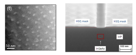
In order to maximize the device performance, engineering of the active material is mandatory. Photonic crystal devices use a perforated membrane which means that surface recombination of carriers and high-temperature operation are important issues. Quantum dots, selective growth and/or buried heterostructures are tools for addressing this. Furthermore, the Bloch-modes in photonic crystal devices potentially allow a tailoring of the overlap between the active material and the optical fields given that accurate spatial and spectral positioning of the material can be done. In NATEC we have addressed the shaping of quantum dots on InP to achieve a desirable level structure and developed selective area growth for accurate positioning of active materials in photonic crystal devices.

Left: Plan-view scanning transmission electron microscope images of sample with QDs. Right: Example of selective area etching and growth of InGaAs on InP.
We work on the following topics:
- Fabrication and characterization of InAs / InGaAsP quantum dots emitting at 1.5 μm
- Selective area growth of quantum wells and quantum wires
Relevant NATEC papers:
S. Kadkhodazadeh, E. S. Semenova, K. Yvind, and R. E. Dunin-Borkowski, “Investigating the chemical and morphological evolution of GaAs capped InAs/InP quantum dots emitting at 1.5μm using aberration-corrected scanning transmission electron microscopy”, J. Cryst. Growth 329, 57–61 (2011).
E. S. Semenova, I. V. Kulkova, S. Kadkhodazadeh, M. Schubert, and K. Yvind, “Metal organic vapor-phase epitaxy of InAs/InGaAsP quantum dots for laser applications at 1.5 μm”, Appl. Phys. Lett. 99, 101106 (2011).
D. Cooper, J.-L. Rouviere, A. Béché, S. Kadkhodazadeh, E. S. Semenova, K. Yvind, and R. Dunin-Borkowski, “Quantitative strain mapping of InAs/InP quantum dots with 1 nm spatial resolution using dark field electron holography”, Appl. Phys. Lett. 99, 261911 (2011).
S. Kadkhodazadeh, E. S. Semenova, M. Schubert, M. Thuvander, K. M. Stiller, K. Yvind, and R. E. Dunin-Borkowski, “Towards quantitative threedimensional characterisation of buried InAs quantum dots”, in 17th international conference on microscopy of semiconducting materials, Vol. 326, 1 (Nov. 2011), p. 012046.
E. S. Semenova, I. V. Kulkova, S. Kadkhodazadeh, M. Schubert, R. E. Dunin-Borkowski, and K. Yvind, “InAs/InGaAsP quantum dots emitting at 1.5 μm for applications in lasers”, in 23rd International Conference on Indium Phosphide and Related Materials (May 2011), pp. 1–4.
N. Kuznetsova, E. Semenova, S. Kadkhodazadeh, M. Schubert, and K. Yvind, “Nano-selective area growth of InGaAs/InP using CBr4 insitu etching”, in Advanced photonics congress (2012), JTu5A.12.
E. Semenova, I. Kulkova, S. Kadkhodazadeh, M. Schubert, E. Stock, and K. Yvind, “Epitaxy of inas/inp quantum dots for device applications at 1.55 μm”, in Semiconductor and Integrated Opto-Electronics Conference (Apr. 2013).
E. S. Semenova, I. V. Kulkova, S. Kadkhodazadeh, D. Barettin, O. Kopylov, A. Cagliani, K. Almdal, M. Willatzen, and K. Yvind, “Epitaxial growth of quantum dots on InP for device applications operating at the 1.55 μm wavelength range”, in SPIE Photonics West, Vol. 8996 (Feb. 2014), p. 899606.
N. Kuznetsova, I. V. Kulkova, E. S. Semenova, N. V. Kryzhanovskaya, A. E. Zhukov, and K. Yvind, “Crystallographic dependent in-situ CBr4 selective nano-area etching and local regrowth of InP/InGaAs by MOVPE”, submitted to J. Cryst. Growth (2014).
Kuznetsova, N. P. Colman, E. Semenova, N. V. Kadkhodazadeh, S and Kryzhanovskaya, S. Ek, W. D. Xuea, M. Schubert, A. E. Zhukov, and K. Yvind, “Nonplanar nanoselective area growth of InGaAs/InP”, Proc. SPIE - Int. Soc. Opt. Eng. 8996 (2014).